“Do you know where your wafers are? Are you SURE?”
This adaptation of the famous public service announcement is as relevant for semiconductor process and industrial engineers as it was (and still is) for responsible parents. Given the ever-present productivity and profitability pressures in modern wafer fabs, it is essential to know the location and status of all product material at all times, because this information drives the scheduling and material delivery systems that provide competitive advantage for the world’s leading manufacturers. Until recently, material visibility at the lot/FOUP level was sufficient for this purpose, but this is no longer the case.

As production managers look for ways to squeeze more capacity out of their existing capital equipment, they realize that a deeper understanding of the wafer processing sequence within a particular tool type may provide opportunities to shorten the its overall lot processing time and increase the amount of material that can be processed simultaneously. The first improvement results from identifying and eliminating unnecessary “wait” states* that individual wafers (or groups of wafers) may experience because of sub-optimal internal material handling, shared resource constraints, mis-calibrated subcomponents, poor recipe design, or a combination of these and other factors. The second improvement results from starting the next lot scheduled for a given tool as soon as all the wafers in the current lot have cleared the first stage of the process. This technique is sometimes called “cascading” or “continuous processing,” and applies to an increasing number of multi-chamber equipment types.
When applied to all the critical “bottleneck” tools in a factory, you can imagine what the resulting benefits would be for cycle time and capacity. Estimates of 3-5% improvement in these KPIs are not unrealistic.
Easy to say, right? But not so easy to implement? Perhaps not as daunting as you think…
The information required to track the precise location, movement, and status of individual wafers in semiconductor manufacturing equipment is most likely available for most equipment types in the form of “events” that chronicle the behavior of substrates, substrate locations, process chambers, aligners, wafer handling robots, and the other equipment components that affect wafer processing. What’s missing is a standard model that unifies this information across multiple equipment types, which would greatly simplify the data collection and analysis software required to implement a robust, generic material tracking system.
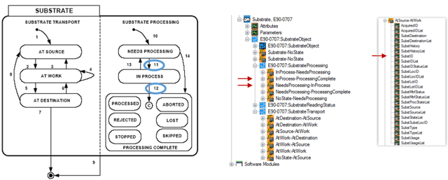
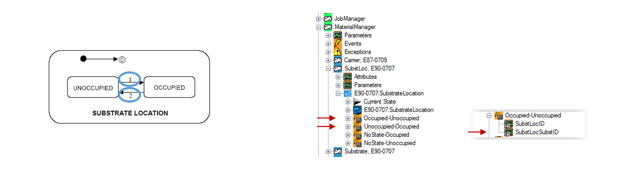
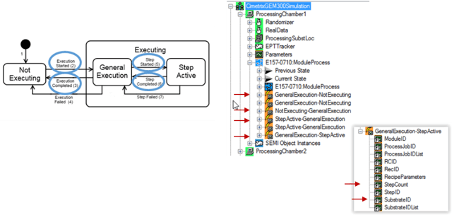
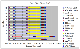
Here, too, the industry standards are actually ahead of today’s “state of the practice.” For example, the SEMI E90 “Substrate Management” and E157 “Specification for Module Process Tracking” standards define all the state machines, transition events, and associated context parameter data necessary to create a detailed Gantt chart of individual wafer movement and processing from start to finish, and allocate each contiguous time segment to its associated “active” or “wait” time element. The insights gained from this sort of visualization point directly to the opportunities cited above for improved tool control and factory scheduling.
Excerpts of these standards, a treeview representation of their respective models, and examples of the potential tracking displays are shown below.
↓
Note that the SEMI E164 “Specification for EDA Common Metadata” calls for the inclusion of E90, E157, and a list of other GEM300 standards in the EDA equipment metadata model, so any E164-compliant equipment would directly and completely support such a material tracking application.
This article is only the second in the series recently announced in the Models in Smart Manufacturing Series Introduction posting – be sure to watch for subsequent postings that will expand on this theme.
We look forward to your feedback and to sharing the Smart Manufacturing journey with you.
*The list of potential “wait” states for semiconductor manufacturing has now been precisely defined and standardized as SEMI E168 “Specification for Product Time Measurement.” The standard also describes how they can be calculated using a specific set of standard material movement events commonly used in 300mm manufacturing equipment.